Mark Hoffman No Comments

Advanced MMICs Aid in Reducing Size and Power in Phased Array Radar Systems

Phased-array radar systems are important instruments in national electronic defense strategies. From the large, ship-based systems that scan for distantly launched missiles to the more compact arrays installed on fighter aircraft and unmanned aerial vehicles (UAVs), electronic phased-array radars come in many sizes and forms, providing reliable signal detection and identification. These modern systems offer many advantages over earlier radar systems that relied on the physical movement of an antenna to steer a radar beam in search of a target. This earlier method is certainly proven and reliable, having been used in military platforms and commercial aviation for over 70 years, but it is limited in scan rate by the mechanical motion of the antenna. In contrast, a phased-array radar system uses many equally spaced antenna elements with phase shifters, with each element contributing a small amount of electromagnetic (EM) radiation to form a much larger beam. As the phase of each antenna element is shifted and aligned, the direction of the radar beam changes and, as the amplitude of each element is varied, the pattern of the far-field response is shaped into the desired response. Thus, the overall radar antenna beam can be steered without need of a mechanically rotated antenna. Beam forming, which can be now performed by means of analog or digital control, can take place at extremely high speeds, limited only by the switching speed of electronic components

Historically, phased-array radar systems have been large in both cost and weight. With the explosive growth of UAVs and unmanned ground vehicles (UGVs) as key elements of the defense arsenal, the need for lighter phased-array radar systems in these weight-sensitive systems will continue to grow. In addition, the increased use of such radars for non-military applications, such as tornado detection by the US National Weather Service (Springfield, MO), is helping drive the demand for lower-cost systems. Fortunately, these growing demands placed on phased-array radar systems can be met with the help of modern RF/microwave integrated-circuit (IC) and monolithic-microwave-integrated-circuit (MMIC) technologies.

PHASED-ARRAY BENEFITS AND DRAWBACKS

The benefits of phased-array radar systems far outweigh their limitations, thus accounting for their growing use in many military electronic systems and platforms. Since beam steering in phased arrays can be performed at millisecond and faster speeds, the signal can jump from one target to the next very quickly, while frequency agility can be used to search quickly across a sector for targets. The coverage of a phased-array antenna beam is typically limited to a 120-deg. sector in azimuth and elevation. While this response is a known limitation of phased arrays, mechanically scanned radar systems also have limitations in the physical area available for the motion of the antenna. Important factors hindering the adoption of phased-array radar systems in many applications continue to be size, weight, power, and cost (SWAP-C). Efforts aimed at minimizing these four attributes represent a significant technological challenge that until recently has seemed a rather formidable hurdle. Phased array radars are, after all, quite complex and even growing in this regard as target identification becomes more difficult. How can SWAP-C reduction be accomplished?

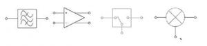
A phased-array radar system (Fig. 1) is constructed from large numbers (often thousands) of transmit/receive (T/R) modules which enable the array to function as both a transmitter and a receiver. Initially designed with discrete hybrid components such as amplifiers, filter, mixers, phase shifters, and switches, these modules are now more commonly fabricated with high-frequency IC or MMIC technology. This switchover to IC technology has provided tremendous benefits in terms of SWAP-C reduction, but simply replacing components can only get a designer so far. Gaining additional SWaP-C benefits in any phased-array radar system also requires knowledge of how to best apply available IC and MMIC technologies to the system (Fig. 2). In fact, the key characteristics of size, weight, and power consumption in a phased-array radar system can usually be minimized by analyzing the design at the circuit, system, and technology levels.

Analysis at the technology level first involves a choice of semiconductor material. Modern commercial semiconductor foundries typically offer a number of different material technologies, but a choice among these is not always straightforward. Components in high-frequency T/R modules typically include high-power amplifiers (HPAs) for transmit purposes, low-noise amplifiers (LNAs) for receiving purposes, mixers and oscillators for signal translation (frequency upconversion and downconversion), and attenuators, filters, and switches for signal conditioning. Fabricating MMICs for all of these functions will likely require more than one semiconductor technology. For example, processes based on silicon-carbide (SiC) or gallium nitride (GaN) substrates will excel in higher-power portions of the system such as transmit functions, while processes using silicon-germanium (SiGe) or gallium-arsenide (GaAs) materials will exhibit lower noise for better performance in receiver functions.

Analysis at the system and circuit levels should be closely intertwined, as a system is only as good as the sum of its components. Unfortunately, the vast majority of IC and MMIC circuit suppliers do not give enough consideration to any specific system, opting instead to create generic components that can be used across wide reaching applications. Such an approach, while cost-effective in terms of IC and MMIC development, is not always optimal in reducing SWaP-C since these components cannot be easily customized for use in phased array systems.

Forward-thinking MMIC suppliers, such as Custom MMIC, have worked on approaches that combine technology, system, and circuit analysis to create components that resolve SWaP-C challenges in phased array systems. At the technology level, they have worked with nearly all of the world’s commercial III-V semiconductor foundries, and have intimate knowledge of some of the newest processes including optical pHEMT and high frequency GaN. At the system level, they have been engaged with numerous phased array designers and have heard first-hand how yesterday’s components are holding back development of next-generation low cost, low weight, high performance systems. At the circuit level, they have created an extensive intellectual property (IP) design library of components in both die and packaged form that are used as a starting point for advanced signal chain design and optimization.

As an example, one place where they have focused significant development is the transmit HPA, a common component required in almost every application. At microwave and millimeter-wave frequencies, the transmit amplifier is often fabricated from a depletion mode pHEMT process, a highly efficient and mature technology. However, depletion mode pHEMT is not without its drawbacks, most notably the need for negative gate voltage and a sequencing procedure to ensure the gate voltage is applied before the drain voltage, lest the FET device suffer irreparable harm. By their very nature, negative voltages and sequencing circuits for HPAs are expensive in terms of complexity, board space, and cost of the extra components. In phased arrays, especially ones with thousands of elements, such HPAs place enormous strain on the system as a whole and offer significant barriers to SWaP-C reduction. Therefore, as part of a Small Business Innovative Research grant (SBIR) from the U. S. Army, they attacked this problem for the transmit portion of an X-band phased array system. Rather than utilize depletion mode pHEMT, they turned to enhancement mode pHEMT for the HPA, a technology often relegated to other applications such as high-speed logic circuitry or switches. In enhancement mode, the pHEMT is normally off until a positive voltage is applied to the gate. Negative voltages are no longer required, nor are voltage sequencers, since either the control or the drain voltage can be applied first; the amplifier will not turn on until both are present. In the end, they were able to replace the existing depletion mode PA with an enhancement mode design that delivered 5 dB more gain, 1 dB more power, and 2 dB improved linearity, all while dissipating 25% less DC power. In terms of SWaP-C, the benefits of enhancement mode PAs are enormous, and offer a significant breakthrough for microwave system designers in general.

A second problem they considered was the receiver LNA in an X-band phased array system as part of a separate SBIR contract. Here, they also switched from a depletion mode to an enhancement mode process, thereby eliminating the negative voltages and sequencers of the existing solution. Their resulting design had 1 dB lower noise figure, 8 dB more gain, an eight-fold reduction in DC power, and half the unit cost of the existing depletion mode solution. However, they soon encountered an application that called for a pair of relatively well-matched LNAs, one for each of the two polarizations in the return signal. Starting with their enhancement mode LNA, they created a dual version on one MMIC die, thereby guaranteeing a matched pair. They also worked with their packaging vendor to develop a low cost rectangular QFN plastic package to best match the resulting die size. The end result was a “standard” product that was anything but ordinary, as it combined innovation at the circuit, system, and technological levels to deliver a component with significant impact on SWaP-C.

Moving forward, they are continuing to develop components for phased array radar systems and similarly challenged 5G wireless systems. Using other technologies such as high frequency GaN, and a combination of different semiconductor devices in multi-chip modules, they’re looking to help designers when digital control functions must be integrated with higher frequency functions.

“We’re learning more everyday about phased array radar and antenna system design challenges,“ says Custom MMIC CSO, Charles Trantanella. “Our product design approach has always been to listen and react, and we’re very pleased to have been able to not only deliver the high frequency performance specifications phased array system designers were looking for, but also the added-value of things like positive bias and positive gain slope characteristics that are proving invaluable in their quest to meet SWaP-C objectives.”

To learn more, download the Tech Brief: “Simplify Amplifier Biasing Using Positive Bias pHEMT MMICs

For application engineering assistance and additional technical resources, visit: https://www.custommmic.com/support

Mark Hoffman No Comments

pSemi Releases World’s First, Fully Integrated, 8-channel LED Boost

Power Supply in Package (PSiP) Uses a Unique Design Based on a Patented, Two-stage Architecture that Relies on Capacitors to Handle the Bulk of the Power-conversion Work

SAN ANTONIO – APPLIED POWER ELECTRONICS CONFERENCE (APEC) – March 6, 2018 – pSemi Corporation (formerly Peregrine Semiconductor), a Murata company focused on semiconductor integration, introduces the PE23300, the industry’s only fully integrated LED boost power supply in package (PSiP) based on a charge-pump, switched-capacitor architecture that offloads most of the power-conversion work from the inductor to capacitors in the charge pump.

Powering up to eight LED strings at a total power level of up to 10 watts, the PE23300 is designed specifically to power LED backlight arrays in ultra-high-definition (UHD) and high definition (HD) LCD panels for 2-cell and 3-cell narrow-voltage DC notebooks, industrial and automotive displays.

“The PE23300 truly demonstrates pSemi’s power-semiconductor capabilities. The PSiP delivers a unique, two-stage architecture that brings ground-breaking conversion efficiency and small solution size and is packaged with Murata’s advanced, 3D-packaging technology and passive components,” says Stephen Allen, director of strategic marketing at pSemi. “All components required for operation are integrated into a 7.7 x 11.7 millimeter laminate-based LGA package, which is just 1.6 millimeters in height. To achieve this small size, we used a ‘die-in-substrate’ 3D-packaging technology. The low profile is also a result of our two-stage architecture that allows us to use a tiny chip inductor. All of this can be achieved with an efficiency that is on average about 5 to 7 percent higher than the competition, halving the losses in the LED boost.”

Power conversion creates a compromise between size and efficiency: The smaller the solution, the worse the efficiency. This compromise impacts OEMs trying to make next-generation, ultra-compact products, because they need both a very high conversion efficiency and a very small size at the same time. pSemi solves this problem with a novel, two-stage architecture that offloads most of the power-conversion work from the inductor to a virtually lossless charge pump and relies on small, multilayer ceramic capacitors (MLCCs) to do most of the work. As a result, the inductor – usually the largest and tallest component – can be reduced dramatically in size, and traditional wire-wound inductors can be replaced with chip inductors. This patented architecture was first developed by Arctic Sand Technologies, an MIT spin-out acquired by pSemi in March 2017, and commercialized this year.

Beyond the smaller inductor and higher efficiency, this architecture delivers several other key benefits for LED boosts, including full short-circuit protection and a very flat efficiency over the entire load range. Also, efficiency is virtually independent of the output voltage, and this allows more LEDs per string. With fewer strings, efficiency is optimized, and the display-bezel size can be reduced in width. pSemi’s PE23300 features low power dissipation – up to half that of competing products – that improves reliability and supports portable applications’ extensive battery run times.

Product Features

The PE23300 features an input voltage range of 4.5V to 15V DC and powers up to eight strings of LEDs at up to 45V and 40 mA per string.

The PSiP provides full programmability via an I2C interface with settings stored in non-volatile memory or by using GPR pins. Dimming resolution is up to 12-bits resolution with an additional 3-bit dithering and can be either linear/logarithmic analog and PWM dimming or direct PWM dimming for maximum flexibility and resolution. The part features an LED brightness ramp up/down control with programmable ramp rate, linear/logarithmic ramp profiles and phase-shifted PWM dimming among active strings to minimize audible noise.

About pSemi 

pSemi Corporation is a Murata company driving semiconductor integration. pSemi builds on Peregrine Semiconductor’s 30-year legacy of technology advancements and strong IP portfolio but with a new mission: to enhance Murata’s world-class capabilities with high-performance RF, analog, mixed-signal and optical solutions. With a strong foundation in RF integration, pSemi’s product portfolio now spans power management, connected sensors, optical transceivers antenna tuning and RF frontends. These intelligent and efficient semiconductors enable advanced modules for smartphones, base stations, personal computers, electric vehicles, data centers, IoT devices and healthcare. From headquarters in San Diego and offices around the world, pSemi’s team explores new ways to make electronics for the connected world smaller, thinner, faster and better. To view pSemi’s semiconductor advancements or to join the pSemi team, visit www.psemi.com.

(News release by pSemi/March news )

Mark Hoffman No Comments

A Perfect Low Noise Amplifier

Low Noise Amplifiers (LNAs) are a critical component in virtually all radar, wireless communications and instrumentation systems. But while the noise figure (NF) performance is often your primary focus, other microwave system considerations related to performance and size, weight, power and cost (SWaP-C) can be equally, if not more important.  We’ll describe a few other key characteristics that may help you save time during your design cycle, save money during assembly, and even enhance your microwave assembly or subsystem at-large.

1. Input Power Survivability

Specifically in military and aerospace radar and communications applications, where electronic countermeasures (ECMs) may be used to overwhelm a receiver, a receiver must be capable of withstanding high levels of input power for varying intervals of time. Active or passive jamming can cause levels of noise and frequency bursts that couple large amounts of broadband or frequency-selective interference into a receiver. Moreover, in these applications there is often a high-power transmitter in close proximity to the receiver, which can lead to substantial coupling and power ingress into the receiver front end.

A common method to reduce the impact of critically high input powers to a receiver is to include a limiter or circulator on the input of a receiver chain. An unfortunate side effect of adding anything prior to the LNA in the receiver is the degradation of the overall system noise figure. These signal chain additions reduce the sensitivity of the receiver, which may shorten communications range, throughput, radar range and accuracy, and cause delays in acquiring mission critical information. A great 1 dB system noise figure can effectively become 2 dB or more when adding protection circuitry.

It’s thus very important to consider an LNA’s highest input power handling (or input survivability). Most LNAs can handle only 10-15 dBm pulsed on their input, but the highest achievers are now surviving 20 dBm continuously and 23-25 dBm pulsed and can help you eliminate the protection circuitry.

2. Gain Flatness, and Gain Stability over Temperature

Gain flatness across your required band is essential to achieve required inter-symbol-interference (ISI) levels and optimal range performance. As costly equalizers are often employed to compensate for the downward gain slope of typical LNAs, positive gain slope LNAs reduce that need.

Another factor to consider is gain stability over temperature. In applications such as aerospace communications, and SatCom, operating temperature can exceed 180 degrees F of variation within a short time window.

Temperature changes that are significant can affect an LNA by more than just changing the noise figure of the device and system; they can vary the frequency-dependent gain of the LNA. For example, large-phased array antennas may have thousands of TR modules, with many of the modules exposed to a variety of temperature gradients. If the communications system relies on gain stability throughout the TR modules, and the LNAs gain stability is temperature dependent, the system may suffer a significant loss in performance.

3. Supply Voltage and Power Consumption

Properly biasing a MMIC amplifier is critical to achieving adequate device performance. Depending upon the particular LNA design, the biasing circuitry could be composed of a positive and negative biasing circuit with temperature compensation. Some LNA MMICs have the biasing and compensation circuitry built in, but a positive and negative voltage supply must be provided to the exact specification for the biasing network to operate properly.

When designing at a system-level for a large RF or microwave assembly, many different voltage supplies may be required. Certain design constraints may also limit the noise and stability performance of those power supplies, which may impact the practical LNA performance due to limited power supply rejection ratio (PSRR). To avoid this, additional circuitry may be used to condition the voltage supplies for a given LNA MMIC. Each of these circuits and connection points introduces a potential failure mode to the voltage supplies, and thus impacts system reliability. These supply-voltage circuits also consume valuable assembly real estate and power, contribute to the overall size/weight of the assembly, add costs, and of course, consume design and test time.

In order to reduce the infrastructure necessary to integrate a MMIC LNA into a microwave assembly, engineers at Custom MMIC have applied innovative circuit-design techniques. The designs they have implemented, which only require a single positive voltage supply, also enable a wide range of voltage input for even greater flexibility. All of the necessary circuitry to properly bias these LNAs is integrated into the MMIC itself. Ultimately, when your MMIC requires only a single positive supply voltage it reduces your bill-of-material, overall system complexity, failure modes, and overall system SWaP-C.

In mobile platforms, including aerospace and satellite communications, power constraints are also a system-wide limitation that often dictates what solutions can be used. Moreover, for these applications, the power requirements of the components directly lead to the overall size and cost of the power generation circuits, and hence, the total system SWAP-C. An example of this concept is seen with satellite communications. The power required by a phased-array antenna must be generated by solar cells mounted on the satellite, which is one of the largest contributing factors of satellite weight and size. As launching satellites costs thousands to tens of thousands of dollars per kilogram, reducing the weight of a satellite system can directly influence the cost-per-bit of high-speed satellite communication services.


What makes for a perfect Low Noise Amplifier (LNA) MMIC for your microwave system? The answer could be right under your noise figure.    (Custommic.com/February News)

Mark Hoffman No Comments

What is a SAW Filter?

Here’s some helpful information about RF/Microwave and SAW filters:

The SAW Filter is a device using surface acoustic wave. A characteristic of the filer is that it can be made small, since Q is high and wavelength is about 5-10 fold of the electromagnetic wave, due to the use of mechanical vibration. Moreover, motion is limited to solid surface, and the filtering function is possible with only the circuit that can control SAW on the surface. Typical SAW filters include: RF SAW Filters, IF SAW Filters, SAW Duplexers, SAW Multiplexer and SAW Resonators.